Dongguan Huaqiang fast circuit board Co., Ltd. Founded in 2010, it is committed to becoming a global one-stop hardware solution provider. Headquartered in Dongguan, it provides hardware solutions for global customers (ODM/IDH) and DMS (PCB).Design, PCB manufacturing, device sourcing and PCBA services.
1. In general
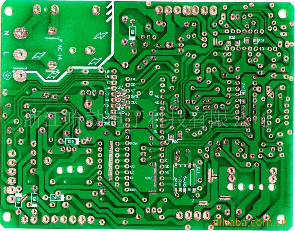
PCB design, because the parasitic capacitance and inductance of the hole have little influence on it, 0.36 mm (aperture) / 0.61 mm (pad) / 1.02 mm (POWER isolation zone) is usually used in the design of the hole of 1-4 layers PCB.A hole in the hole. For special requirements of signal lines, such as power lines and ground wires, 0.41mm/0.81mm/1.32mm holes are usually used.
2. Passing holes are part of the design of printed circuit board (PCB). The function of passing holes is to connect, fix and locate components. A through hole consists of three parts: the pad area around the hole, the POWER isolation zone. Fabrication of through holes:A layer of metal is plated on the cylindrical surface of the hole wall, which is used to connect the copper foil of each layer in the middle. The upper and lower sides of the hole are made into welded discs, and the direct lines are connected (or can be disconnected).
3, through hole is generally divided into three categories: blind hole, buried hole and through hole. Blind holes - located on the top and bottom surfaces of printed circuit boards, with a certain depth (aperture and hole depth in a certain ratio), for the connection of surface and inner circuits. buryHole - the connecting hole in the inner layer of the circuit board (not visible on the surface of the circuit board). Through hole - through the entire circuit board, generally do the positioning and installation of components.The diameter of through hole is 8mil (0.2mm), which is the diameter of mechanical drilling; if it is blind or buried, the diameter is 4mil (0.1mm), which is to be perforated by laser. The smaller the hole, the more expensive it is. 10/18 is recommended for through-hole.12/20 hole, power hole can be 16/24.
The processing of power supply and ground wire makes the wiring in the whole PCB board very well, but the interference caused by the improper consideration of power supply and ground wire will degrade the performance of the product, and sometimes even affect the success rate of the product. placeIn order to ensure the quality of products, the wiring of electric and ground wires should be taken seriously, and the noise interference caused by electric and ground wires should be minimized. For every engineer engaged in the design of electronic products, it is clear that the noise between the ground wire and the power supply line is noisy.The reason for the sound production is only to reduce the noise suppression: it is well known that decoupling capacitors are added between the power supply and ground wires. As far as possible, widening the power supply and the width of the ground wire, preferably the ground wire is wider than the power line width.Ground wire > power line > signal line, usually the width of signal line is 0.2-0.3 mm, the finest width can reach 0.05-0.07 mm, and the PCB of power line is 1.2-2.5 mm, which can form a circuit with wide ground wire for digital circuit.The ground network is used (analog circuit ground can not be used like this) with a large area of copper layer for the ground wire, in the printed circuit board, the unused places are connected with the ground as the ground wire. Or made of multi-storey boards.These are the precautions for Huaqiang fast
PCB hole design. If you don't understand, you can ask our website's online customer service staff.
