PCB copy price is based on the following points reported as well as PCB board ten steps, Huaqiang Fast Electronics can be based on the prototype clone development, for engineers, research and development institutions to provide learning and research information. The PCB copy board team, which has over 10 years of practical experience in board, ensures the success rate of the copy board and provides circuit boards.
One-stop PCB board copying solutions such as board modification, schematic diagram copying, chip model identification, chip decryption, PCBA substitutes and so on!
PCB needs to be evaluated before copying.
1, is there an encryption program?
2, is there a polished model and a fake chip?
3, is there a device for shutting down production or other factors that make it difficult to purchase?
Note: the above three items can not be solved, will affect the success rate of the copy board!!!
PCB copy board needs to provide:
Simple single and double panels need to provide a set of templates, if it is multi-layer, can provide two sets of exactly the same template;
PCB copy board we can give the following information:
PCB files (or Gerber files), bill of materials (BOM) files, schematic files;
Kanban, the higher the number of layers, the higher the price of PCB.
Look at the size, the size of the board!
Look at the quantity, the more the price will drop.
Ten steps of
PCB copying board
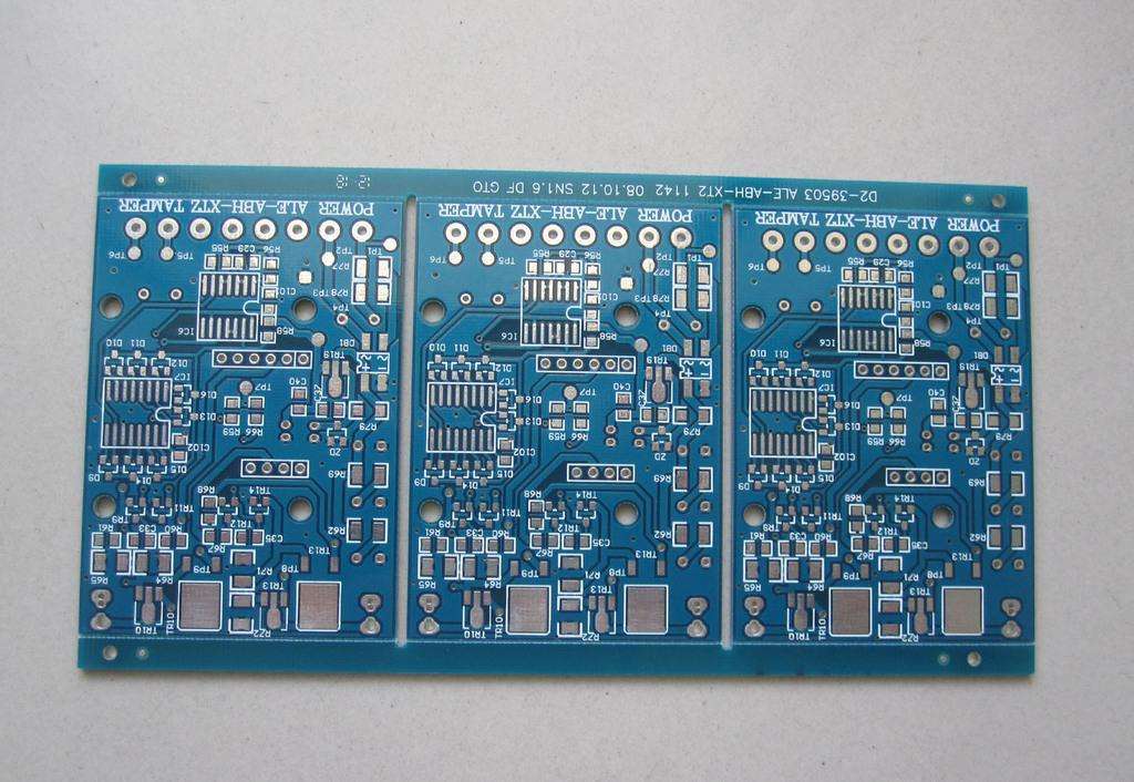
The first step is to get a piece of PCB. First, record the type, parameters, and position of all the components on paper, especially the direction of diodes, triodes, and the direction of the IC gap. It is better to scan out the position of two pieces of gas with a scanner, which is very helpful to restore the prototype in the future.
The second step is to remove all the devices and remove the tin from the PAD hole. Wash the PCB empty board with ultrasonic wave, then put it into the scanner. Note that the PCB must be horizontal and straight in the scanner. Otherwise, the scanned image can not be used. Then open the Photoshop software to input the scanner. After the scanner starts, the DPI resolution can be set according to the density. If set is 600DPI. Use the color method to sweep the silk screen and save the name to customize it. The bottom screen printing method is the same.
In the third step, the two layers of TOP LAYER and BOTTOM LAYER are slightly ground with water yarn paper, then polished to the bright copper film, put into the scanner, start the PHOTOSHOP software, sweep the two layers in color and save. Note that PCB must be leveled straight in the scanner.
Fourth, adjust the size of the canvas, contrast, brightness, so that there is a strong contrast between the part with copper film and the part without copper film, and then turn the second picture into black and white, check whether the line is clear, if not clear, then repeat this step. If it is clear, save it as black and white BMP format TOP.BMP and BOT.BMP.
Fifth, the two BMP format files are converted to PROTEL format files, in PROTEL into two layers, such as two layers of PAD and VIA overlap basically, indicating that the previous steps do well, if there are deviations, then repeat the fourth step of the third step.
Step 6: Convert TOP. BMP to TOP. PCB. Be careful to convert to the SILK layer, which is the Yellow layer. Then you trace the line in the TOP layer and place the device according to the drawings in step 2. Delete the SILK layer after drawing.
The seventh step is to BOT. BMP was converted to BOT. PCB, pay attention to the SILK layer, which is the light yellow layer, and then you line it on the BOT level. Delete the SILK layer after drawing.
The eighth step is to include TOP in PROTEL. PCB and BOT. When PCB is transferred, it becomes a OK.
The ninth step, the same as the middle layer of the board copy process, repeat steps 6-7, the final output of the PCB file, is a multi-layer together with the same physical PCB diagram
Step 10: Compare the original image to the 1:1 file on the PCB board, and if you're right, you're done. Huaqiang fast circuit board Co., Ltd. is a very professional board company.
PCB copy board prices are based on the following newspapers and
PCB board 10 steps explained here today. Next time have the opportunity to share with you.