1.
PCB proofing or batch production, surface treatment and process are as follows
Cutting is the process of cutting the original copper clad or fiberglass board into a board that can be made on a production line.
Now let's look at three concepts:
(1) SET: SET refers to the Engineer in order to improve the production speed, convenient production and other reasons, the number of UNIT together a whole figure. That's what we often call the puzzle board, which includes unit graphics and process edges.
(2) UNIT:UNIT refers to the individual cell graphic designed by PCB design engineer.
(3) PANEL: PANEL refers to the PCB manufacturer in order to improve the speed, convenient production and other reasons, the SET together with a tool board edge, composed of a board.
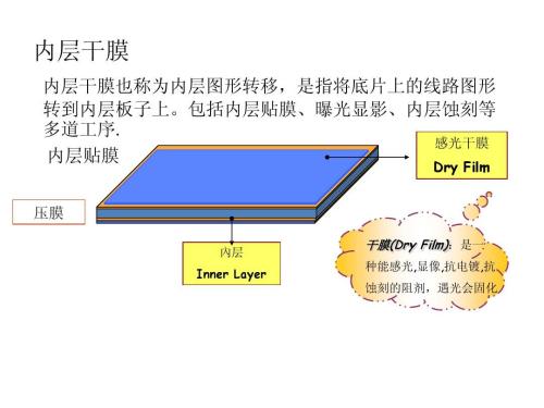
2. inner layer dry film (INNER DRY FILM)
The inner layer dry film is the process of grafting the inner line pattern onto the PCB board.
In PCB production we will mention the concept of graphics grafting, because PCB production is fundamentally conductive graphics production. So there is a very important link in the process of graphic grafting for PCB production.
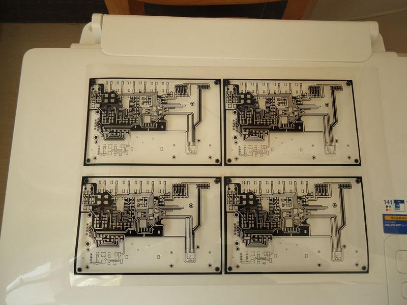
The inner layer dry film includes exposure development, inner layer film, inner layer etching and so on. The inner layer is a special layer of photosensitive film on the surface of the copper plate. This film will solidify in the light and form a protective film on the board. Exposure development is the exposure of a film-coated plate, the light transmission part will be cured, the non-light transmission part or the previous dry film. Then, after developing, the dry film was dried off, and the plate covered with solidified protective film was etched. After the film is removed, the inner layer of the circuit will be transferred to the circuit board. The whole process is as follows.
For professional designers, the most important consideration is the widths, spacing control and wiring uniformity. Because too small spacing will cause film clipping, membrane can not be faded short circuit. The line width is too small, and the adhesive force of the membrane is not enough. Therefore, the safe spacing in circuit design (including wire and pad, wire and wire, pad and pad, wire and copper surface, etc.) must be considered in production.
(1) pretreatment: grinding plate
The main role of grinding plate: basic pretreatment is to solve the problem of surface roughness and surface cleanliness. Removal of oxidation increases copper surface roughness and facilitates film attachment on copper surface.
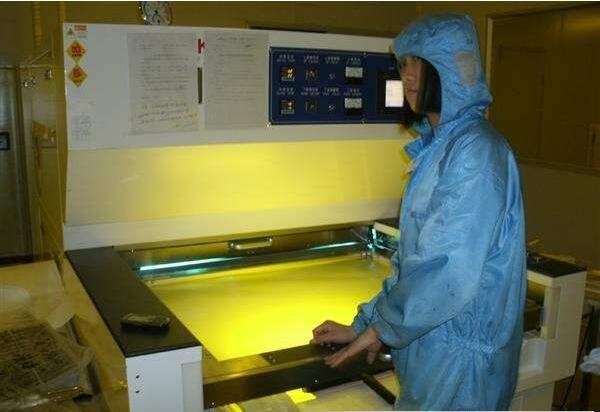
(2) exposure
The film is aligned with the pressed dry film substrate, and the pattern of the film is transferred to the sensitive dry film by ultraviolet irradiation on the exposure machine.
(3) patch
Dry film or wet film is pasted on the treated substrate by hot pressing or coating to facilitate subsequent exposure production.
(4) etching
Unexposed dry/wet film is removed by developer and exposed to copper surface. The exposed copper surface is dissolved and corroded with acid copper chloride to obtain the desired circuit.
(5) film withdrawal will protect the exposed surface of the copper surface from the sodium hydroxide solution and reveal the line pattern.
(6) development
Unexposed dry/wet films are dissolved and washed away by the weak alkalinity of the developer (sodium carbonate) and the exposed parts are retained.
3 laminates
Lamination is the process of bonding all layers of circuits into a whole by virtue of the adhesion of PP sheets. This bonding is achieved by the diffusion and infiltration of macromolecules at the interface, resulting in interweaving. The discrete multilayer plate and the PP sheet are pressed together to form the required number of layers and thickness of the multilayer plate. Copper foil, bonded sheet (semi-solidified sheet), inner plate, stainless steel, isolation plate, kraft paper, outer plate and other materials will be overlapped according to the process requirements.
Symmetry is the first consideration for designers. Because the plate will be affected by pressure and temperature in the lamination process, there are stresses in the plate after lamination. Therefore, if the two sides of the laminated plate are not uniform, the stress on the two sides is different, causing the plate to bend to one side, greatly affecting the performance of PCB.
In addition, even in the same plane, if the distribution of copper cloth is not uniform, the resin flow rate will be different at different points, so that the place with less copper cloth will be slightly thinner, and the place with more copper cloth will be slightly thicker.
In order to avoid these problems, the uniformity of copper distribution, lamination symmetry, blind buried hole design layout and other factors must be considered in detail.
4, brownish
Objective: to form a micro rough and organic metal layer on the inner surface of copper and enhance the cohesion between layers.
Process principle:
A uniform organic metal layer structure with good adhesion property is produced by chemical treatment. The surface of the copper layer is controlled to coarsen before the inner layer is bonded. It is used to enhance the bonding strength between the inner layer of copper and the semi-cured sheet.
5. Drilling
A through hole is generated between the layers of the circuit board to achieve the purpose of connecting layers.
Legendary drill tools
6. Copper plate plating
(1) copper precipitation.
Also known as chemical copper, the drilled PCB plate in the copper cylinder oxidation-reduction reaction, the formation of copper layer and pore metallization, so that the original insulating substrate surface deposition of copper, to achieve interlayer electrical connectivity.
(2) plate plating
The PCB plate just deposited copper is thickened to 5-8um on the surface and in the hole to prevent the thin copper from being oxidized and slightly eroded in the hole before the graphic electroplating.
7. Outer layer dry film.
Same as the inner layer dry film process.
9, outer layer plating, SES
The hole and line copper layer are plated to a certain thickness (20-25um) to meet the requirements of the final copper thickness of PCB sheet. And etching the bare copper surface.